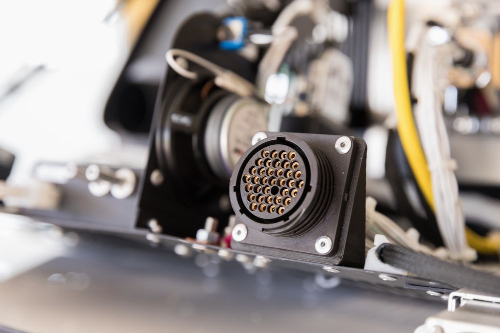
Designing a multilayer PCB can feel like a puzzle where every connection counts. At first glance, vias seem like minor details. They’re just tiny holes linking layers. But those decisions ripple across signal integrity, board real estate, and long-term reliability. Each via type carries trade-offs. Understanding how and when to use them leads to cleaner layouts, faster builds, and fewer production surprises.
What Is a Via in a PCB?
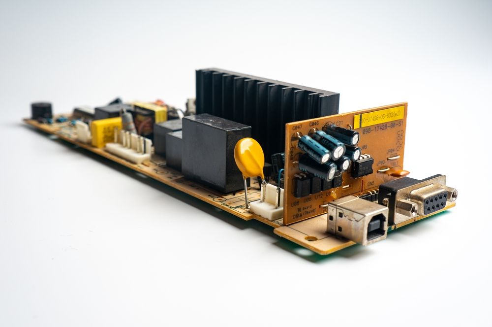
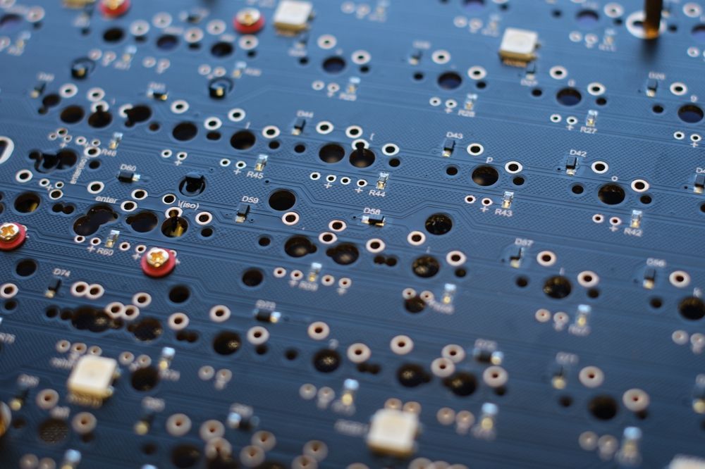
A via is a small, drilled hole that connects different layers of a printed circuit board. It allows electrical signals and power to travel between layers without disrupting the board’s compact layout. In multilayer designs, vias make it possible to route complex interconnects while maintaining signal performance. They're formed during the drilling and plating stages of PCB fabrication. While small in size, their placement and type can have a large impact on cost, performance, and manufacturability, especially in high-speed, high-density, or reliability-focused designs.
Overview of the Different Types of PCB Vias
Each via type serves a specific role in routing signals and managing space across layers. Understanding the common types of vias helps engineers make informed layout and manufacturing choices.
Through-Hole Vias (THVs)
Through-hole vias are the most common type and extend from the top layer to the bottom layer of the PCB. They’re typically used in less space-constrained designs or where higher current-carrying capacity is required. THVs are easy to manufacture and cost-effective, making them a go-to for standard multilayer boards.
However, they occupy valuable routing area on all layers and can create signal integrity challenges in high-speed or impedance-sensitive applications. Despite this, they remain widely used in both prototyping and full-scale production.
Blind Vias
Blind vias connect an outer layer of the PCB to one or more inner layers without going through the entire board. This makes them ideal for designs where board space is limited and layer density is high.
By reducing via depth, blind vias help preserve routing area on internal layers and minimize parasitic effects that can impact signal quality. They are more complex to fabricate than through-hole vias, requiring precise depth control, but bring clear benefits in compact, high-performance layouts.
Buried Vias
Buried vias connect two or more internal layers of a PCB without reaching the outer surfaces. They allow designers to increase layer count and routing density without consuming space on the top or bottom layers. Because they are hidden within the board stack, buried vias can help maintain clean outer-layer layouts for critical components, high-speed signals, or impedance-sensitive traces.
These vias require sequential lamination during fabrication, which increases manufacturing complexity and cost. Still, they’re often necessary in tightly packed, multilayer designs.
Microvias
Microvias are small, laser-drilled vias typically used in high-density interconnect (HDI) PCBs. They usually connect only adjacent layers and have a much smaller diameter than mechanically drilled vias. This allows for tighter trace routing, improved signal integrity, and more design flexibility in compact devices like medical instruments or aerospace modules.
Microvias are especially valuable in designs requiring fine-pitch components or multiple high-speed signal layers. Though more expensive to produce, their performance advantages often justify the added cost in demanding applications.
Skip Vias
Skip vias connect non-adjacent layers while intentionally bypassing the intermediate ones. They are often used in high-density PCBs where space is limited, and design constraints prevent routing through each sequential layer. Skip vias are created using laser drilling and typically appear in advanced HDI stackups. Their main advantage is routing efficiency. They allow connections that avoid congested inner layers.
However, their fabrication requires careful planning and process control, which adds to manufacturing cost. They are best suited for compact, multilayer boards requiring advanced layout strategies.
Via-in-Pad (VIPs)
Via-in-pad places the via directly beneath a surface-mount component pad, saving space and shortening the signal path. This is especially useful for high-speed or high-frequency designs where minimizing inductance and improving thermal performance are priorities. VIPs are common in dense layouts that use fine-pitch BGAs or RF components.
To prevent solder wicking, these vias are usually filled and capped during manufacturing. While they simplify routing in tight areas, VIPs increase fabrication cost and require coordination between layout and assembly teams.
Backdrilled Vias
Backdrilled vias are through-hole vias that have unused stub portions mechanically removed after plating. These stubs can act like antennas at high frequencies, causing signal reflections or loss. Removing the unused sections improves signal integrity in high-speed digital designs, particularly those using differential pairs or controlled impedance traces.
This technique is often used in aerospace, networking, or defense systems where clean signal paths are essential. Backdrilling adds processing time and cost but can be critical for meeting strict performance requirements.
Choosing the Right Via for Your PCB Application
Selecting the right via type depends on the design’s electrical, mechanical, and manufacturing requirements. High-speed signals may benefit from microvias or backdrilled vias, while simple multilayer boards can rely on traditional through-hole options.
Space constraints often push designers toward blind, buried, or via-in-pad configurations for improved layout efficiency. Each choice affects not only layout but also yield, testability, long-term reliability, and production cost.
Evaluating the application’s signal integrity needs, layer count, component density, and thermal performance early in the process helps avoid costly revisions and delays later.
Cost, Complexity, and Manufacturability of Via Types
Not all vias are created equal when it comes to fabrication time and production cost. Through-hole vias are the most cost-effective and easiest to produce, but they take up space on every layer.
Blind and buried vias offer space savings but require sequential lamination, which adds steps and cost. Microvias and via-in-pad options involve laser drilling and filling processes that demand tight process control.
Backdrilling is a post-processing step, typically reserved for high-speed applications where clean signal paths justify the extra effort.
How EI Sales Helps Optimize Your PCB Via Strategy
EI Sales connects OEMs to PCB manufacturing solutions that balance technical performance, cost, and production speed. As a trusted partner to both engineers and procurement teams, we help translate design intent into manufacturable outcomes.
Our
PCB design services support early-stage concepts, complex via stackups, and quick-turn prototyping. When comparing
PCB vs. PCBA
needs, we help clarify the scope and align resources accordingly.
We work across medical, aerospace, and industrial programs to support projects at any production stage.
Contact us to talk about your next board.